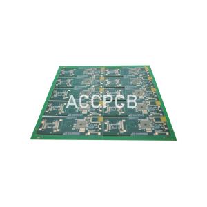
1.30mm thickness PWB Circuit Board 0.2 Mm line Spacing for Car Navigation System Module
Key Specifications/Special Features:
| Layer count : | 4 layer FR4 TG170 |
| Finish thickness : | 1.30 ±10%mm |
| Minimum width/spacing : | 0.2 / 0.2 mm |
| Minimum via dia : | 0.2mm |
| Surface finish : | Immersion gold |
| Solder mask : | Green |
| Legends : | White |
| Certification : | ISO UL ROHS SGS |
| Outline: | Routing,V-Groove, Beveling punch |
Advantages:
▪ No MOQ, 14 years of PCB turnkey services
▪ Quick turn, prototype, low & medium & high volume
▪ OEM services provide
▪ ISO 9001-, ISO 14001-, ISO/TS16949, ISO 13485, IATF16949, OHSAS18001 certified
▪ 100% E-test, visual, AOI inspection, including X-ray, 3D microscope
▪ Fast response within 24 hours
Full range of testing services:
▪ AOI, function testing, In circuit testing
▪ 3D paste thickness test
▪ Flash testing and earth bonding tests can also be undertaken where required
▪ Using our X-ray machine, we test PCBs to component level and all wiring is fully inspected and tested
▪ Each board is carefully examined by our dedicated inspection team using AOI and high magnification viewers
FAQ:
1. What kinds of boards can ACCPCB process?
Common FR4, high-TG and halogen-free boards, Rogers, Arlon, Telfon, aluminum/copper-based boards, PI, etc.
2. What data are needed for PCB production?
PCB Gerber files with RS-274-X format.
3. What’s the typical process flow for multi-layer PCB?
Material cutting → Inner dry film → inner etching → Inner AOI → Multi-bond→ Layer stack up Pressing → Drilling → PTH → Panel Plating → Outer Dry Film → Pattern Plating → Outer etching → Outer AOI → Solder Mask → Component Mark → Surface finish → Routing → E/T → Visual Inspection.
4. How many types of surface finish ACCPCB can do?
the leader has the full series of surface finish, such as: ENIG, OSP, LF-HASL, gold plating (soft/hard), immersion silver, Tin, silver plating, immersion tin plating, carbon ink and etc. .. OSP, ENIG, OSP + ENIG commonly used on the HDI, we usually recommend that you use a client or OSP OSP + ENIG if BGA PAD size less than 0.3 mm.
5. What are the main factors which will affect the price of PCB?
Material;
Surface finish;
Board thickness, Copper thickness;
Technology difficulty;
Different quality criteria;
PCB characteristics;
Payment terms;
6. How do ACCPCB ensure quality?
Our high quality standard is achieved with the following.
1.1 The process is strictly controlled under ISO 9001:2008 standards.
1.2 Extensive use of software in managing the production process
1.3 State-of-art testing equipments and tools. E.g. Flying Probe,e-Testing, X-ray Inspection, AOI (Automated Optical Inspector) .
1.4.Dedicated quality assurance team with failure case analysis process